ProtoLaser H4 – more functions in a compact housing

The ProtoLaser H4, with a laser for structuring tasks and additional mechanical tools, is the link between pure laser devices and the mechanical structuring of circuit boards. The latest version makes some processes even more efficient and expands the range of applications.


The LPKF ProtoMats have been the benchmark for decades when it comes to chemical-free structuring of circuit board prototypes. The spectrum ranges from the smallest system for occasional work to the top model, which uses high spindle speeds to gently process even sensitive substrates.

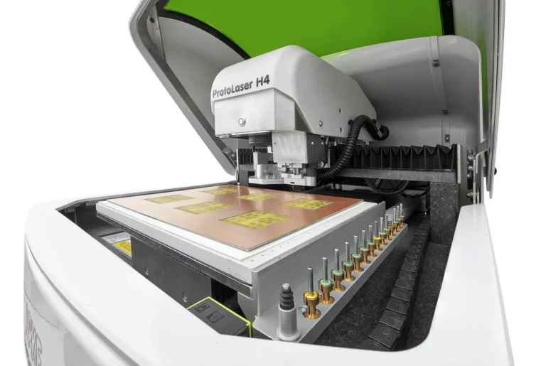
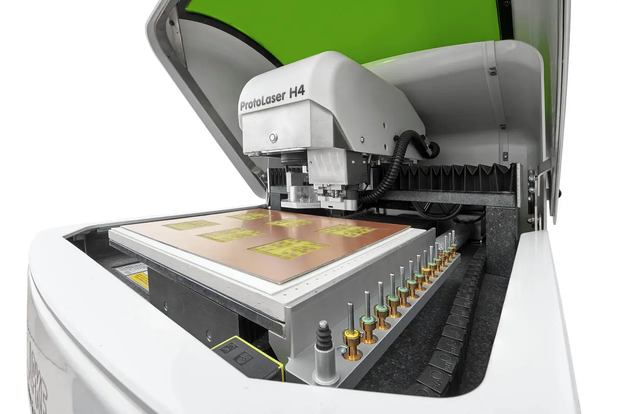
The ProtoLaser H4 has so far been the link between mechanical PCB processing and LPKF laser processes. It can drill or cut mechanically thick substrates and multilayers using mechanical tools and combines this with the extremely fast and precise laser processing. The whole thing fits into a modern tabletop housing. In combination with the associated system software LPKF CircuitPro, even sophisticated prototypes can be produced in your own laboratory without etching chemistry.

With the new revision of the ProtoLaser H4, LPKF is consistently continuing this concept. The laser used has got a 25 percent increase in performance from 16 to 20 watts. Two important improvements have been implemented for mechanical structuring: The number of tool holders has grown from 6 to 14 in order to achieve a higher level of automation without manual tool changes. At the same time, LPKF has increased the spindle speed from 60,000 rpm to 100,000 rpm. This reduces mechanical processing times and enables, for example, 0.2 mm holes and faster separation of PCBs and flexible materials.


The environment around the two processing methods has also improved. The resulting material residues are completely removed from the work area thanks to an optimized extraction hood. An integrated MTM device (Material Thickness Measurement) records the height of the material. This reliably improves the focus position for laser structuring in a self-calibrating process. The z-height raised to 8 mm, so that the working area now grows to 310 mm x 230 mm x 8 mm. The diagonal travel speed has been increased again.

A new camera feature can now read any geometric shape on the circuit board as a registration mark. Any processing steps can be created from these positions. An extended version of the CircuitPro software is available for these features, which also includes export to the most important CAD data formats such as Gerber and DXF.

“In addition to faster and more precise structuring results, we also wanted to expand the range of applications. Thanks to the new features, the LPKF ProtoLaser H4 is also well suited for circuit board repair, for example,” explains LPKF Product Manager Eric Scheidler.

25 Years ProtoLaser: From Vision to Precision Revolution in Electronics Manufacturing

LPKF celebrates silver anniversary of its pioneering laser systems for PCB prototyping

What began in 1989 as a research project between LPKF Laser & Electronics SE and the University of Hannover has developed into one of the most successful product series of the German laser technology company: The ProtoLaser family celebrates its 25th anniversary in 2025. Since the market launch of the first commercial ProtoLaser system in 2000, LPKF has continuously revolutionized laser structuring of printed circuit boards, setting new standards in electronics prototype development. 

“The ProtoLaser has fundamentally changed how research institutions and companies develop electronics prototypes,” explains Lars Führmann. “What started 25 years ago as a simple IR laser system for copper processing is today a diverse product family ranging from UV lasers to picosecond systems that can precisely process virtually any material in the electronics industry.” 

From Beginnings to High Technology 

The success story began in 2000 with the first commercially viable ProtoLaser, which still worked with an external laser source and the ProtoMat 95s system. Just four years later, the ProtoLaser 100 followed as the first system, with an integrated scanner and diode pumped solid state laser. In 2008, the ProtoLaser S was introduced, the first system with scan field stitching for large processing areas. The real breakthrough came in 2012 with the ProtoLaser U3 – the “game changer” featuring the first-ever possible rubout technology with UV laser for large area removal. 

The latest generation comprises four specialized systems: The ProtoLaser U4 with UV laser (over 300 units sold), the ProtoLaser S4 with 532 nm (green) laser with PCB drilling capability (nearly 150 systems deployed), the revolutionary ProtoLaser R4 with 1.5-picosecond pulse length for “cold ablation” without heat-affected zones, and the ProtoLaser H4 for the fastest circuit structuring combined with mechanical processing targeting also thick PCBs and multilayer stacks. 

Technology Leap to Atomic Precision 

“Our technological development reflects the increasing demands of the electronics industry,” Lars Führmann continues. “While in 2000 we still hoped to cut copper without burning too much substrate, today we work with picosecond pulses at the atomic level through multiphoton effects. This evolution from thermal to virtually thermal-free processes has opened up completely new application fields.” 

Today’s ProtoLaser family encompasses a broad material spectrum, ranging from classic FR4 circuit boards to RF substrates, PTFE, polyimide, ceramics, glass, and even graphene and ITO-coated glass. The systems enable structure widths as low as 15 micrometers and processing areas of up to 229 x 305 mm. 

Shaping the Future 

For the next 25 years, LPKF sees further innovation potential: “We are already developing the next system generation and exploring new laser technologies. The increasing miniaturization of electronic components and new material requirements will open up additional possibilities for us,” announces Lars Führmann.