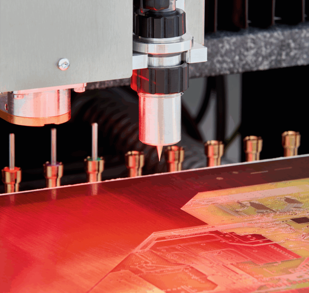
Precise, automated in-house PCB prototyping through high-speed milling, drilling, and engraving – turning your circuit designs into real boards within hours.
Drilling
Milling
Sensor controlled
2.5D prototyping
Low maintenance
Easy-to-use package
Material & copper thickness measurement
Auto tool change – up to 20 tools
Integrated dispenser (optional)
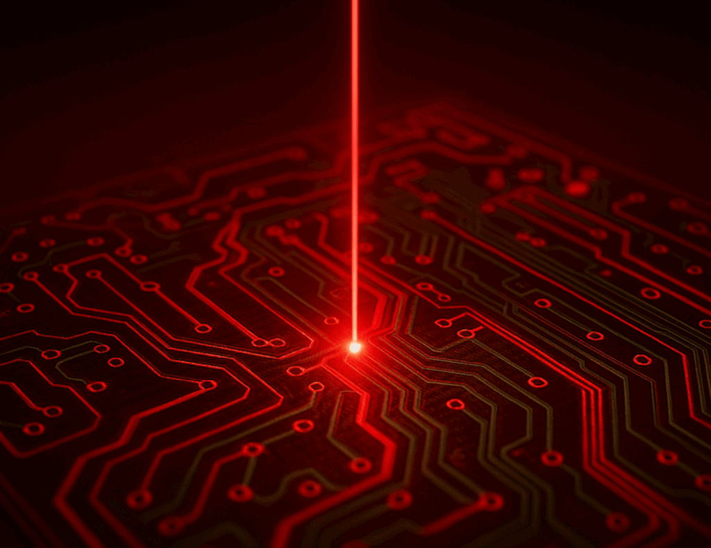
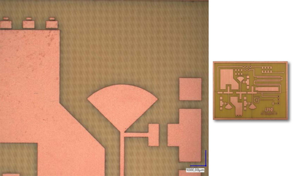
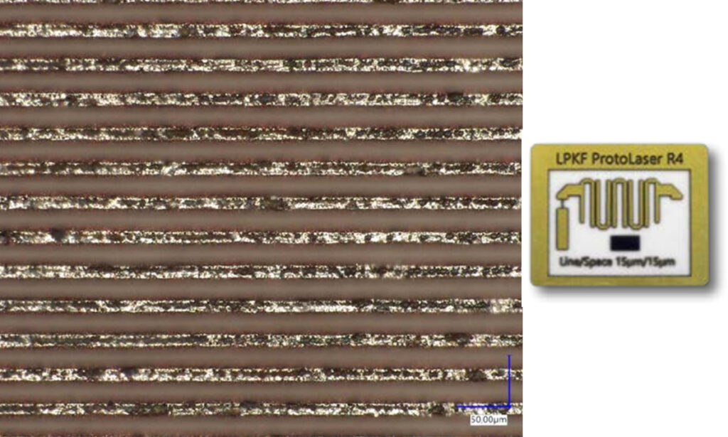
ProtoLaser Series
High-precision laser structuring system with different laser wavelengths and pulse frequencies designed for rapid prototyping and micromachining of PCBs, metals, and advanced materials.
Infrared Laser – high versatility and suited for cutting, engraving, and structuring metallic or hybrid substrates.
Green Laser – Ideal for antenna patterning, and precise copper removal with minimal substrate damage.
UV Laser – Excellent for non-metallic materials requiring clean ablation and fine detail, including RF circuits, flexible electronics, and thin-film patterning.
Picosecond Laser – Extremely fine feature definition with minimal thermal impact; used for research labs, micro-optics, biomedical devices, and semiconductor substrates.
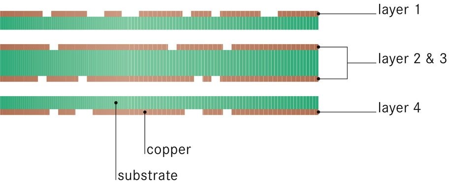
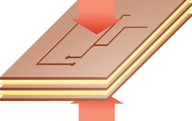
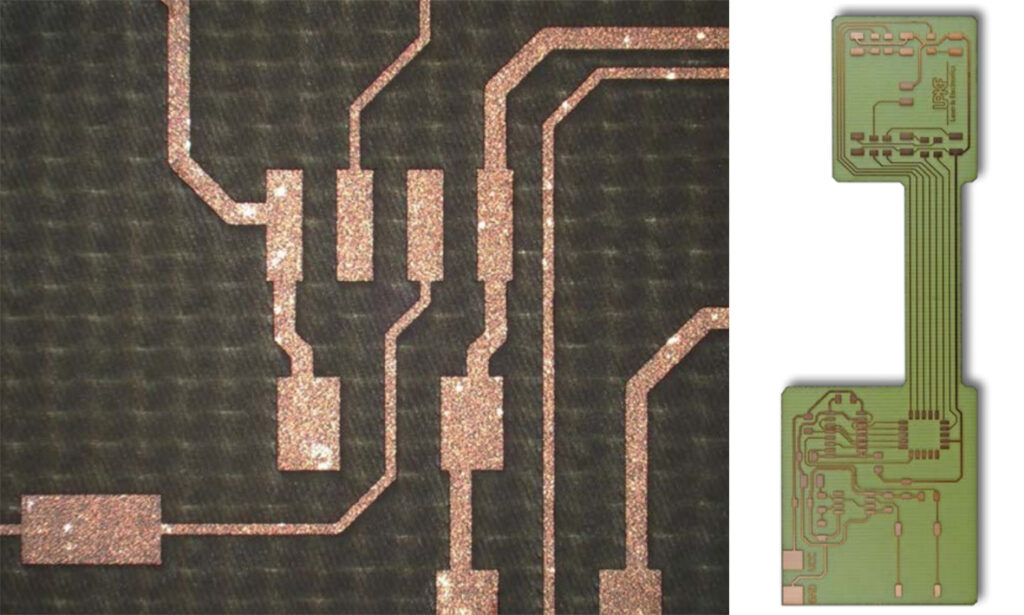
Multi-layer solutions for PCB Prototyping
Production of up to eight layers in-house
A multilayer is made up of multiple layers that are laminated together to form a printed circuit board. The outer layersof a multilayer are usually single-sided PCBs, whereas the inner layers are double-sided materials. Insulating layers, so-called prepregs,are inserted between the conductive layers. Up to four layers can be through-hole plated in a chemical-free process. For electrical connection of up to eight layers through-hole electroplating is recommended.
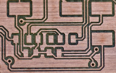
An LPKF ProtoMat or ProtoLaser structures circuit traces directly from layout data, using automatic tool changing and camera-based fiducial alignment to process each layer with minimal manual intervention.
Lamination
The structured layers are stacked with prepregs that provide insulation and bond during lamination. The LPKF hydraulic press system delivers reliable lamination (even for HF multilayers) using preset process profiles.
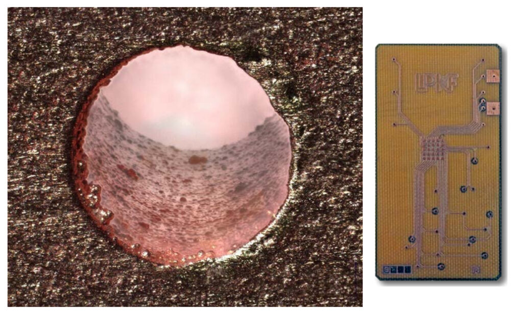
Through-hole plating
Interlayer electrical connections complete the conductor structure. The through-holes are drilled and then metallized using a chemical-free conductive paste; for boards with more than four layers, conventional electroplating is recommended.
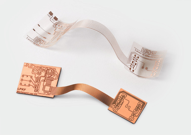
PCB Prototyping Add-ons
PCB process add-ons extend your in-house prototyping from basic structuring to full production-grade functionality. They enable plated vias, durable surface protection, and clean assembly without outsourcing.
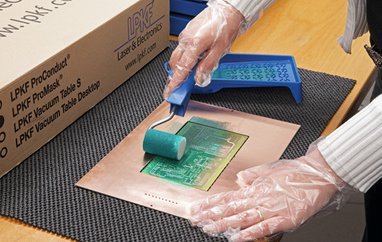
ProConduct
LPKF ProConduct is a system for chemical-free through-hole coating of double-sided and multilayer PCBs with paste. It is compact, fast, and easy to use.
Contac S4
For the wet chemical process, no knowledge of chemistry is needed; the LPKF Contac S4 system independently indicates the necessary process steps.
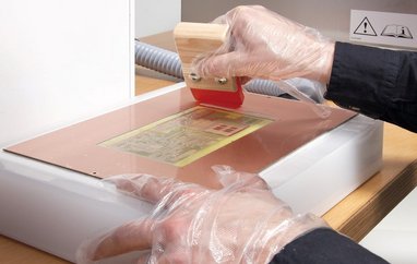
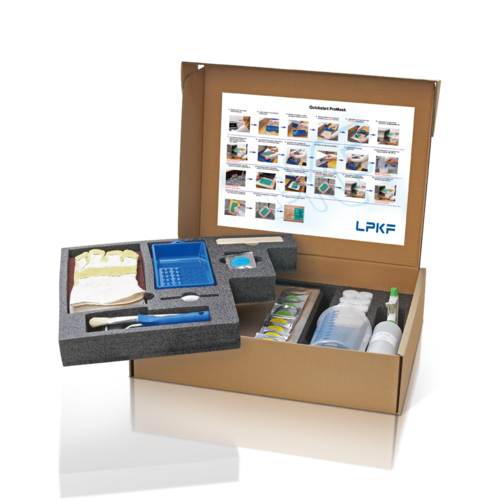
ProMask
Apply a durable solder mask in-house to protect copper surfaces, improve solderability, and achieve a clean, professional PCB finish.
ProLegend
Add high-contrast component markings directly to your prototype for clear identification and smooth, error-free assembly.
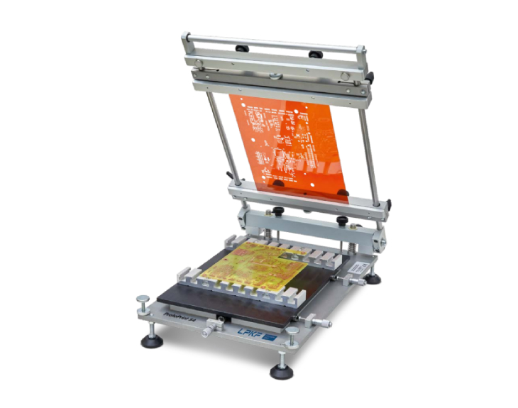
ProtoPrint S4
Screen-printing solder paste with consistent volume and alignment, ProtoPrint S4 ensures reliable SMD assembly on prototype PCBs.
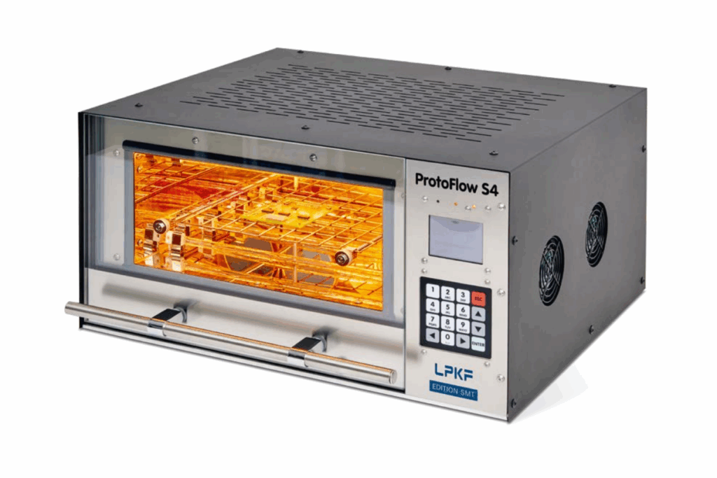
ProtoFlow S4
A controlled reflow environment ensures consistent soldering quality, bringing your SMD assemblies to production-grade reliability.
Electronics Manufacturing
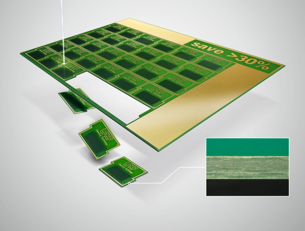
PCB Depaneling
Laser depaneling is the most innovative technique for separating PCB from the panel and is differentiated from the classic separation methods in particular by its flexibility and stress-free processing.
Stress-free processing
High precision and clean edges
Contact-free operation
Minimal heat-affected zone
Support diverse materials
Flexible cutting geometry
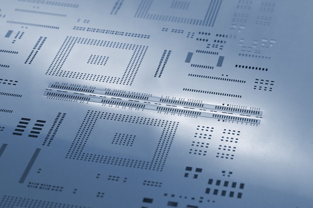
Stencil Cutting
Stencil apertures with defined properties are essential for perfect solder printing results. LPKF StencilLasers are capable of cutting sheets from 20 μm up to 1 mm.
High edge quality for better paste release
Exceptional precision and repeatability
Burr-free and clean cuts
No mechanical stress
Support fine-pitch components
Fast, tool-less production
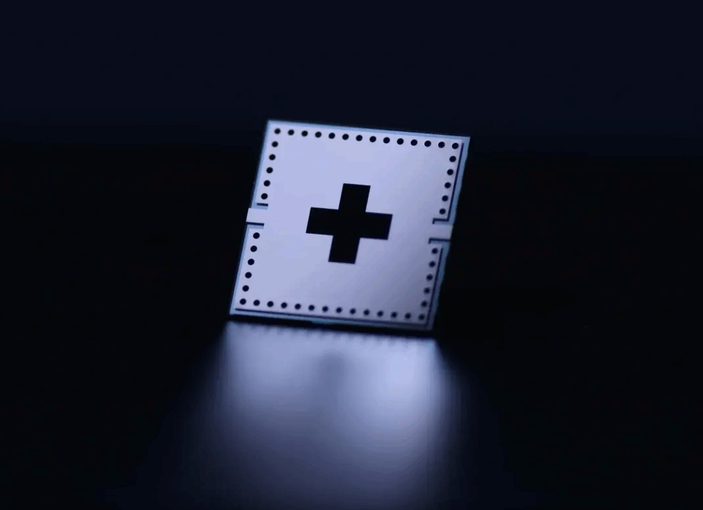
Laser Plastic Welding
Joining plastic components in a way that is precise, reliable, and permanent – without adverse chemical, thermal, mechanical effects on the surrounding material? This is a simple job for LPKF laser welding machines!
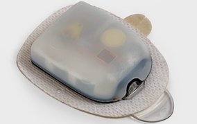
Medical Device
From lab-on-chip systems to catheter and device housings, the process eliminates adhesives, prevents contamination, and ensures full regulatory monitoring.
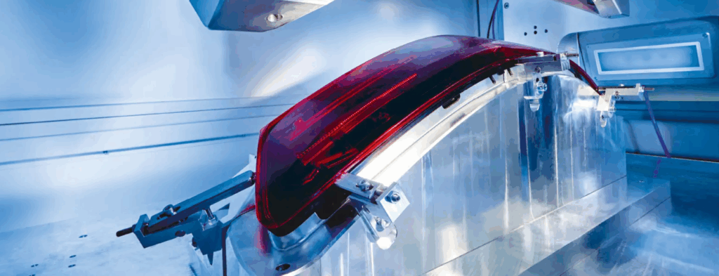
Automotive Components
Welding of sensor housings, vehicle lighting modules, door‐lock assemblies, reservoir tanks, etc.
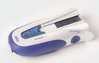
Consumer Products
Small, complex plastic assemblies such as smartphone casings, headphones, VR goggles, consumer appliances.
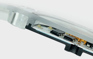
Electronics Housing
Waterproof PCB lighting housings have tight, hermetic seals around the PCB and lighting electronics.
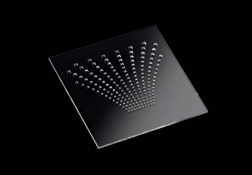
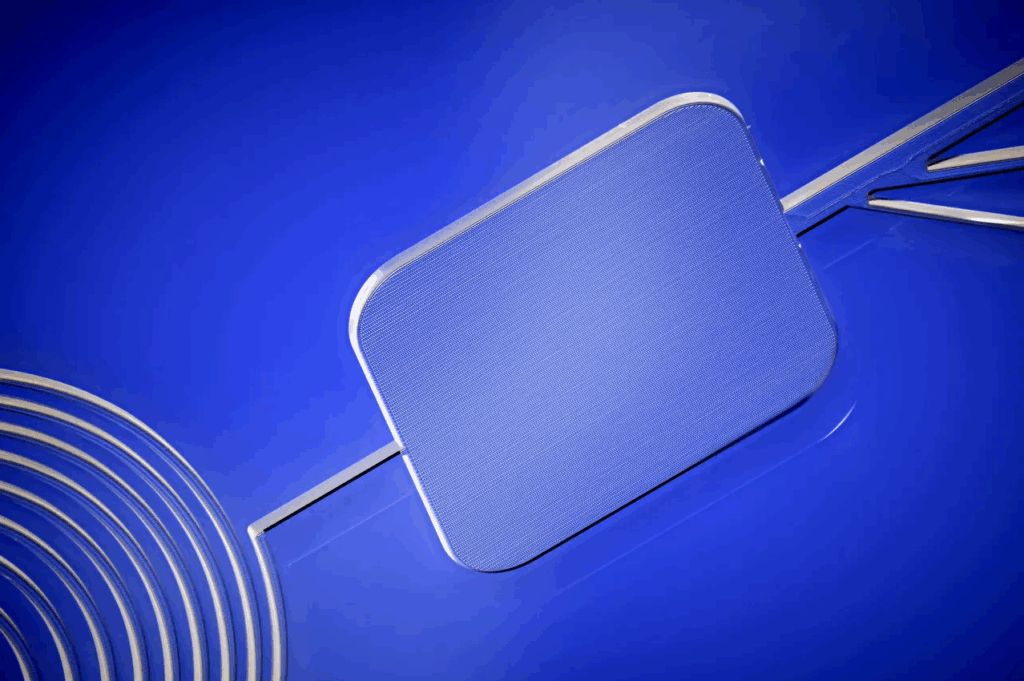
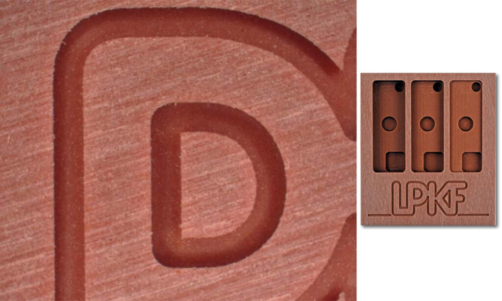
Glass Micro-structure Processing
The LIDE® technology (Laser Induced Deep Etching) developed by LPKF is a new enabling technology for a wide range of applications in microsystems technology —— unlock zero-defect glass processing for your industry’s biggest challenges.